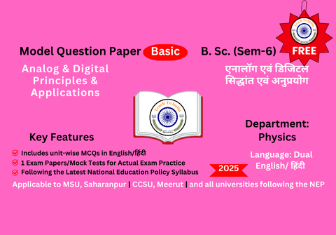
Analog & Digital Principles & Applications - एनालॉग एवं डिजिटल सिद्धांत एवं अनुप्रयोग
- Description
- Curriculum
- Reviews

Model Question Paper
Analog & Digital Principles & Applications – एनालॉग एवं डिजिटल सिद्धांत एवं अनुप्रयोग
Key Features | मुख्य विशेषताएँ
- Bilingual Model Paper | द्विभाषी मॉडल पेपर
- Enough MCQ for Practice | अभ्यास के लिए पर्याप्त MCQ
- Exam Practice Paper with Mock Tests | मॉक टेस्ट के साथ परीक्षा अभ्यास पत्र
- Latest Syllabus as per NEP | NEP के अनुसार नवीनतम पाठ्यक्रम
- Designed by Experts | विशेषज्ञों द्वारा तैयार किया गया
The given MCQs cover only 10% of the syllabus | दिए गए बहुविकल्पीय प्रश्न केवल 10% पाठ्यक्रम को कवर करते हैं।
To cover 100% of the syllabus with summaries, upgrade to our Advanced Model Paper.| पूरा सिलेबस और सारांश कवर करने के लिए हमारा एडवांस मॉडल पेपर जॉइन करें। Join Advanced Model Paper
|
Program Class: Degree / B.Sc. |
Year: Third |
Semester: Sixth |
||
|
Subject: Physics |
||||
|
Course Title: Analog & Digital Principles & Applications |
||||
|
Course Learning Outcomes: 1. Study the drift and diffusion of charge carriers in a semiconductor. 2. Understand the Two-Port model of a transistor. 3. Study the working, properties and uses of FETs. 4. Comprehend the design and operations of SCRs and UJTs. 5. Understand various number systems and binary codes. 6. Familiarize with binary arithmetic. 7. Study the working and properties of various logic gates. 8. Comprehend the design of combinational and sequential circuits.
|
||||
|
Credits: 4 |
Core Compulsory / Elective |
|||
|
Max. Marks: –25+75 |
Min. Passing Marks: 33 |
|||
|
Unit |
Topics |
|||
|
|
Part A: Analog Electronic Circuits |
|||
|
I |
Semiconductor Junction: Expressions for Fermi energy, Electron density in conduction band, Hole density in valence band, Drift of charge carriers (mobility & conductivity), Diffusion of charge carries and Life time of charge carries in a semiconductor. Work function in metals and semiconductors. Expressions for Barrier potential, Barrier width and Junction capacitance (diffusion & transition) for depletion layer in a PN junction. Expressions for Current (diode equation) and Dynamic resistance for PN junction.
|
|||
|
II |
Transistor Modeling: Transistor as Two-Port Network. Notation for dc & ac components of voltage & current. Quantitative discussion of Z, Y & h parameters and their equivalent two-generator model circuits. h-parameters for CB, CE & CC configurations. Analysis of transistor amplifier using the hybrid equivalent model and estimation of Input Impedance, Output Impedance and Gain (current, voltage & power).
|
|||
|
III |
Field Effect Transistors: JFET: Construction (N channel & P channel); Configuration (CS, CD & CG); Operation in different regions (Ohmic or Linear, Saturated or Active or Pinch off & Break down); Important Terms (Shorted Gate Drain Current, Pinch Off Voltage & Gate Source Cut-Off Voltage); Expression for Drain Current (Shockley equation); Characteristics (Drain & Transfer); Parameters (Drain Resistance, Mutual Conductance or Transconductance & Amplification Factor); Biasing w.r.t. CS configuration (Self Bias & Voltage Divider Bias); Amplifiers (CS & CD or Source Follower); Comparison (N & P channels and BJTs & JFETs). MOSFET: Construction and Working of D-MOSFET (N channel & P channel) and E-MOSFET (N channel & P channel); Characteristics (Drain & Transfer) of D-MOSFET and E-MOSFET; Comparison of JFET and MOSFET.
|
|||
|
IV |
Other Devices: SCR: Construction; Equivalent Circuits (Two Diodes, Two Transistors & One Diode-One Transistor); Working (Off state & On state); Characteristics; Applications (Static switch, Phase control system & Battery charger). UJT: Construction; Equivalent Circuit; Working (Cutoff, Negative Resistance & Saturation regions); Characteristics (Peak & Valley points); Applications (Trigger circuits, Relaxation oscillators & Sawtooth generators).
|
|||
|
|
PART B: Digital Electronics |
|||
|
V |
Number System: Number Systems: Binary, Octal, Decimal & Hexadecimal number systems and their inter conversion. Binary Codes: BCD, Excess-3 (XS3), Parity, Gray, ASCII & EBCDIC Codes and their advantages & disadvantages. Data representation.
|
|||
|
VI |
Binary Arithmetic: Binary Addition, Decimal Subtraction using 9’s & 10’s complement, Binary Subtraction using 1’s & 2’s compliment, Multiplication and Division.
|
|||
|
VII |
Logic Gates: Truth Table, Symbolic Representation and Properties of OR, AND, NOT, NOR, NAND, EX-OR & EX-NOR Gates. Implementation of OR, AND & NOT gates (realization using diodes & transistor). De Morgan’s theorems. NOR & NAND gates as Universal Gates. Application of EX-OR & EX-NOR gates as pairty checker. Boolean Algebra. Karnaugh Map.
|
|||
|
VIII |
Combinational & Sequential Circuits: Combinational Circuits: Half Adder, Full Adder, Parallel Adder, Half Substractor, Full Substractor. Data Processing Circuits: Multiplexer, Demultiplexer, Decoders & Encoders. Sequential Circuits: SR, JK & D Flip-Flops, Shift Register (transfer operation of Flip-Flops), and Asynchronous & Synchronous counters.
|
|||
-
1Unit 1: MCQs - Analog & Digital Principles & Applications
-
2Unit 2: MCQs - Analog & Digital Principles & Applications
-
3Unit 3: MCQs - Analog & Digital Principles & Applications
-
4Unit 4: MCQs - Analog & Digital Principles & Applications
-
5Unit 5: MCQs - Analog & Digital Principles & Applications
-
6Unit 6: MCQs - Analog & Digital Principles & Applications
-
7Unit 7: MCQs - Analog & Digital Principles & Applications
-
8Unit 8: MCQs - Analog & Digital Principles & Applications


